
20 min read ·
A Technical Guide to the Chiplet Architecture and Hybrid Bonding Paper
The official SMTA proceedings text is restricted. Find the DOI, compare secondary copies and resolve which publication date belongs in your citation.
Paper access, citation, authors, and publication chronology
Citation and access
Title: “The Future of Electronics Packaging Is Chiplet Architecture” DOI: 10.37665/smCTRSC40814 Publication: SMTA International, volume 27, pages 82–92 Document type: Conference paper Version of record: Official SMTA proceedings record
The official SMTA record identifies the work as a conference paper in SMTA International, volume 27, pages 82–92, and gives an online-publication date of October 19, 2025. It supplies the authoritative DOI, abstract, author list, page range, copyright notice, and publisher-controlled access route. The full proceedings text is marked as restricted access.
The ten listed authors are:
- Pavanbabu Arjunamahanthi
- Himanandhan Reddy Kottur
- Shajib Ghosh
- Patrick J. Craig
- M. Shafkat M. Khan
- Liton Kumar Biswas
- Istiaq Firoz Shiam
- Navid Asadizanjani
- Robert Patti
- Charles Woychik
Available metadata associates the first eight authors with the University of Florida and Robert Patti and Charles Woychik with NHanced Semiconductors. Name rendering varies slightly across records: the official page uses “Patrick Craig,” while another index includes the middle initial, and the company-hosted manuscript reverses the displayed order of Istiaq Firoz Shiam’s name. A definitive bibliography should follow the official record or the title page of the version being cited rather than silently normalizing an index entry.
A conventional engineering-style citation is:
P. Arjunamahanthi, H. R. Kottur, S. Ghosh, P. J. Craig, M. S. M. Khan, L. K. Biswas, I. F. Shiam, N. Asadizanjani, R. Patti, and C. Woychik, “The Future of Electronics Packaging Is Chiplet Architecture,” SMTA International, vol. 27, pp. 82–92, 2025, doi: 10.37665/smCTRSC40814.
Exact punctuation, abbreviation, capitalization, and treatment of the online-publication date depend on the required citation style. The essential elements are the complete author list, paper title, venue, volume, page range, year, and DOI.
Primary and secondary access routes
The SMTA proceedings page is the version of record. It should be the starting point for authoritative metadata, access status, and any publisher-issued corrections.
NHanced Semiconductors provides an author-affiliated landing page and a company-hosted paper copy. The NHanced paper page labels the item “Technical Paper, September 24, 2025” and says Charles “Chuck” Woychik presented it at SMTA International in Rosemont, Illinois. This is a useful secondary route, but readers should not assume that a company-hosted file has the same status as the proceedings version.
ResearchGate provides another secondary access path, including an uploaded copy and citation export. Its record warns that uploaded content may be subject to copyright. Readers should verify the file’s version and applicable permissions before reproducing or redistributing it; repository availability does not make a copy the version of record.
Why several dates appear
The dates associated with the paper describe different events:
- September 24, 2025: the date assigned to the technical paper on the NHanced company page.
- October 1, 2025: the publication date shown by the Semantic Scholar index record.
- October 19, 2025: the online-publication date on the official SMTA proceedings page.
- March 18, 2026: the date on which ResearchGate says the displayed author content was uploaded to its platform, according to the repository record.
These dates can correspond to preparation, presentation, indexing, proceedings publication, or repository upload. They should not be collapsed into one chronology. For a definitive citation, use the official SMTA metadata and the rules of the relevant citation style rather than substituting an index date or repository-upload date.
What the paper argues—and what it does not establish
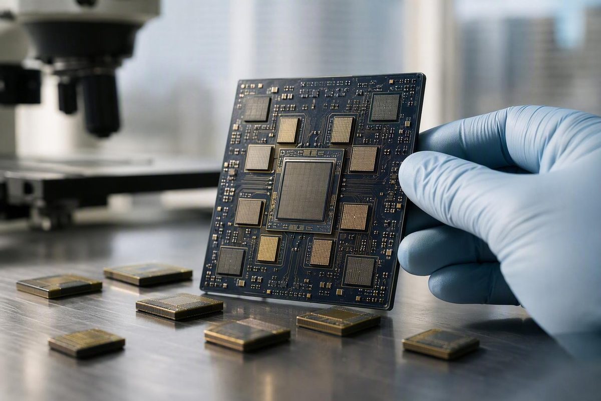
A chiplet is an independently fabricated functional die designed to be integrated with other dies in one package. Rather than placing every system function on one monolithic piece of silicon, a chiplet architecture partitions those functions across multiple dies and reconnects them through package-level interfaces.
The paper’s architectural case begins with modularity. One package can combine logic, memory, analog, RF, and I/O dies fabricated using process technologies suited to their functions. Leading-node logic might be paired with memory or I/O made on processes selected for density, voltage handling, analog behavior, maturity, or cost. The package consequently becomes a system-integration platform, not merely a protective enclosure.
The paper identifies greater functionality, heterogeneous integration, scalability, and improved performance per watt as drivers of this transition. It also treats high-density, low-latency interconnects as central to integrating multiple chiplets. The accessible company-hosted manuscript describes the work as a technical roadmap and process assessment for hybrid bonding in fine-pitch chiplet packaging.
Two concepts must remain distinct:
- Chiplet architecture is a system-design and partitioning strategy.
- Hybrid bonding is a physical assembly and interconnect method that can join dies or wafers.
A chiplet system does not inherently require hybrid bonding. Depending on pitch, bandwidth, latency, cost, thermal conditions, compatibility, and production requirements, it may use micro-bumps, an interposer, a bridge, an organic redistribution structure, direct bonding, or another package technology.
Why the interfaces matter
Partitioning moves communication that would otherwise occur through on-die wiring onto die-to-die interfaces. This creates an architectural exchange: modularity and process flexibility are gained, but additional physical and protocol boundaries are introduced.
Those boundaries can add resistance, capacitance, power consumption, latency, and area overhead. A chiplet package succeeds only if its interconnects provide sufficient bandwidth, energy efficiency, signal integrity, and reliability for the intended workload.
Shorter and denser connections can reduce some interface penalties, which is why hybrid bonding occupies a central place in the paper. Physical pitch alone, however, cannot determine complete-system performance.
An evidence-limitations note
The paper’s title states the authors’ forward-looking position. It does not prove that chiplets will replace every monolithic system-on-chip or that one package architecture will dominate every market.
This guide assessed the publisher’s bibliographic record and abstract together with the accessible company-hosted manuscript material represented in the supplied evidence. That material includes the process roadmap and quantitative comparison table, but the available extract is incomplete and does not provide a sufficient basis to determine consistently which figures came from original experiments and which were synthesized from cited literature.
The numerical values discussed below must therefore be treated as paper-reported comparisons, not independently reproduced results. A stronger assessment would require the complete methods, reference list, material stacks, sample counts, test geometries, equipment, statistical treatment, and uncertainty analysis.
Why chiplets are attractive—and when monolithic designs still win
Chiplet adoption is driven by several related pressures: diminishing returns from conventional transistor scaling, rising advanced-node cost and complexity, the greater defect sensitivity of large dies, practical lithographic reticle limits, and demand for functions that do not all benefit equally from the newest process technology.
A modular design can address those pressures conditionally through:
- Process-node flexibility: each function can use a suitable fabrication process.
- Reuse: a validated die can be incorporated into multiple products.
- Known-good-die selection: dies can be screened before package assembly.
- Modular updates: one function can be revised without redesigning every block.
- Scalability: multiple dies can create a system larger than one practical monolithic die.
- Heterogeneous integration: logic, memory, analog, RF, photonic, or specialized dies can be combined where their technologies and interfaces are compatible.
A Cadence system-design discussion likewise identifies smaller-die yield, reuse, node flexibility, and known-good-die purchasing as potential benefits. It also emphasizes that achieving them requires package-aware connectivity, verification, testing, and electrothermal analysis across chips, interposers, packages, and boards. The Cadence chiplet white paper cautions that ecosystem development and cross-domain design flows remain necessary.
A known-good die is only known to have passed the tests and operating conditions applied before assembly. It can still be damaged during handling, placed incorrectly, bonded incompletely, or found defective when operated with other dies under package-level stress.
Application areas
The paper discusses artificial intelligence, high-performance computing, data-center systems, high-bandwidth memory, image sensors, and logic-memory integration. These are plausible targets because they may demand large aggregate silicon area, specialized processing, extensive memory bandwidth, or close integration of different technology types.
Not every implementation benefits equally. Suitability depends on:
- workload communication patterns;
- required memory capacity and bandwidth;
- die-to-die traffic;
- latency tolerance;
- thermal-density limits;
- production volume;
- process availability;
- input-die yield;
- test strategy; and
- package and cooling cost.
An architecture suited to a large data-center accelerator may be inappropriate for a compact, low-power product with stringent cost, standby-power, or qualification requirements.
2.5D and 3D integration
In 2.5D integration, dies sit side by side and connect through an interposer, bridge, redistribution structure, or related package substrate. Its disadvantages can include larger package area, additional substrate cost, and longer links than a vertical stack.
In 3D integration, dies are stacked vertically. Stacking can shorten selected connections, increase integration density, and bring logic closer to memory. It can also complicate heat extraction, power delivery, mechanical stress, inspection, test, and rework.
Neither geometry is intrinsically superior. Many systems combine lateral and vertical integration.
The costs of disaggregation
A chiplet strategy introduces burdens that monolithic designs avoid or reduce:
- Die-to-die links add electrical and protocol overhead.
- Advanced substrates, interposers, bridges, or bonding steps can increase package cost.
- Each die and interface requires verification and test coverage.
- Final yield depends on assembly quality as well as input-die quality.
- Multiple heat sources complicate thermal management.
- Power delivery must control droop and noise across several dies.
- Warpage and mechanical stress can affect alignment and reliability.
- Multi-vendor sourcing creates interoperability and accountability questions.
- Product schedules may depend on multiple foundries, assemblers, IP owners, and test flows.
The commercial outcome therefore depends on the whole system. Savings from die reuse or smaller dies can be offset by expensive packaging, low assembly yield, demanding cooling, or long qualification cycles.
Where monolithic integration remains compelling
Monolithic integration can remain preferable when the design prioritizes:
- minimal communication latency;
- extremely tight functional coupling;
- compact physical area;
- low interface power;
- simpler design and verification;
- mature qualification procedures;
- lower package complexity; or
- clear supply and failure ownership.
An imec comparison of chiplets and monolithic ASICs reaches a coexistence-oriented conclusion: chiplets are attractive for large, heterogeneous, modular, or reticle-constrained systems, while monolithic designs remain suitable where simplicity, latency, tight coupling, size, or low power dominate.
The evidence therefore supports coexistence among monolithic, 2.5D, and 3D designs—not universal replacement.
How hybrid bonding differs from micro-bump assembly
Hybrid bonding creates direct copper-to-copper and dielectric-to-dielectric interfaces. At the bonded interface described by the paper, it does not use the solder bumps, inter-bump underfill, or comparatively tall interconnect stack associated with conventional micro-bump assembly.
At a simplified physical level:
- Micro-bump assembly uses raised conductive features joined through thermocompression or a related bonding process. The spaces around the features may be filled with underfill for mechanical support and environmental protection.
- Hybrid bonding prepares very flat copper and dielectric surfaces so that the dielectric regions establish intimate contact and the aligned copper features form electrical connections, with annealing supporting the final interface.
Eliminating the solder-bump geometry can reduce interconnect height and permit finer pitch. The paper attributes lower parasitic resistance, capacitance, and latency to shorter connections and higher connection density.
Paper-reported values
The following values are taken from the accessible paper material. They are not independently validated production results, and the underlying cited studies, test conditions, geometries, materials, sample sizes, and uncertainty data were not available for assessment in the supplied evidence.
| Metric | Hybrid bonding: paper-reported value | Micro-bumps: paper-reported value |
|---|---|---|
| Interconnect pitch | Below 10 µm | At least 30 µm |
| Interconnect stack height | At or below 5 µm | 20–30 µm |
| Thermal interface resistance | Approximately 1.2 mm²·K/W | Approximately 8–15 mm²·K/W |
| Current-density handling | Above 8.9 MA/cm² | Approximately 1.5–5 MA/cm² |
These figures are reproduced in the paper’s accessible comparison table and should be interpreted as paper-reported values rather than universal process limits.
Pitch may describe a design target, demonstrated test vehicle, process capability, or production rule. Thermal interface resistance depends on the measured stack, contact area, materials, boundary conditions, and test method. Current-density limits depend on copper geometry, temperature, duty cycle, failure criterion, and test duration. Stack-height comparisons are meaningful only when both columns include equivalent structures.
The defensible conclusion is narrow: under the conditions represented by the paper’s sources, hybrid bonding can provide a shorter and finer-pitch interface than conventional micro-bumps. The table does not establish higher final-package yield, lower lifecycle cost, better workload performance, commercial-volume maturity, or longer service life.
The five-step hybrid-bonding process
The paper organizes the hybrid-bonding flow into five phases:
- Surface planarization
- Cleaning and surface activation
- Die alignment
- Low-temperature bonding
- Post-bond annealing
Each phase establishes conditions needed by the next. Because the process depends on intimate contact across dielectric regions and very small copper features, surface or placement errors that might be tolerated by a coarser interconnect can become critical.
1. Surface planarization
Chemical mechanical planarization, or CMP, levels the copper pads and surrounding dielectric. The goal is controlled relative height, low roughness, and acceptable uniformity across the bonding surface.
Excessive copper dishing can leave copper recessed below the dielectric. Across-die or across-wafer height variation can create regions that bond successfully and others that remain separated.
Planarization control therefore addresses:
- copper dishing and erosion;
- local and global nonuniformity;
- surface roughness;
- pad-height variation;
- dielectric topography; and
- compatibility with subsequent cleaning and activation.
2. Cleaning and surface activation
Cleaning removes particles, organic residue, process chemicals, and other contamination. Activation prepares the dielectric surface to establish the intended initial bond.
The relevant chemistry and activation method depend on the copper, dielectric, equipment, and integration flow. The paper’s high-level roadmap should not be treated as a universal recipe for every material stack.
3. Die alignment
Alignment registers opposing copper features. As pitch decreases, the allowable overlay error also shrinks.
The paper reports better than 500 nm overlay accuracy for wafer-to-wafer alignment and states that chip-to-wafer placement may require sub-200 nm precision at pitches below 5 µm. These are paper-described requirements or capabilities, not guarantees for every tool or production line. The same paper describes post-bond annealing as typically occurring at 200–300°C.1
Chip-to-wafer alignment can be especially demanding because each die must be picked, handled, oriented, measured, and placed. Edge damage, backside contamination, and geometric variation can affect position or coplanarity even when the die remains electrically functional.
4. Low-temperature bonding
The prepared surfaces are brought into contact so that the dielectric regions establish the initial bond.
“Low temperature” is relative to the integration flow and its thermal budget. It does not identify one universal temperature or imply that the entire process occurs at room temperature. Incomplete contact can leave voids or unbonded regions, while particles or topographic variation can obstruct uniform propagation of the bond front.
5. Post-bond annealing
Annealing strengthens the interface and supports copper connection through solid-state diffusion. The applicable temperature and duration remain material- and process-dependent.
Thermal exposure can introduce stress where materials have different expansion behavior. It must also remain compatible with dielectric layers, passivation, previously fabricated devices, and other temperature-sensitive package structures.
Hybrid bonding is cumulative: final quality depends on control of every preceding phase.
Process-to-risk map
| Process phase | Primary objective | Representative failure risks |
|---|---|---|
| Surface planarization | Create coplanar copper and dielectric surfaces | Copper dishing, erosion, roughness, height variation, nonuniformity |
| Cleaning and activation | Remove contamination and prepare bondable surfaces | Particles, residue, oxidation, corrosion, inadequate activation |
| Die alignment | Register opposing interconnect features | Overlay error, rotation, distortion, edge damage, loss of coplanarity |
| Low-temperature bonding | Establish intimate dielectric contact and initiate the interface | Voids, trapped contamination, incomplete contact, local debonding |
| Post-bond annealing | Strengthen the bond and complete the copper connection | Thermomechanical stress, delamination, material degradation |
The phases are difficult to decouple during failure analysis. Effective process control therefore requires traceable metrology at several stages rather than inspection only after bonding is complete.
Chip-to-wafer versus wafer-to-wafer integration
Hybrid bonding can follow several assembly paths. Two principal options are chip-to-wafer and wafer-to-wafer bonding. Neither is categorically better; each changes the balance among flexibility, throughput, yield, equipment requirements, and product architecture.
Chip-to-wafer bonding
In chip-to-wafer assembly, individual dies are selected and placed onto a target wafer or larger structure. The incoming dies can differ in size, function, fabrication technology, or source wafer, making the method attractive for heterogeneous integration.
A major benefit is the ability to select known-good dies before placement. Screening can reduce the probability that an already detected defective die consumes package area and assembly resources. It is particularly valuable when a package contains expensive or scarce components.
Pre-bond screening does not guarantee a working final package. Assembly can introduce contamination, misalignment, edge damage, incomplete bonding, or electrical defects. Some failures emerge only when the dies operate together or experience package-level thermal and mechanical stress.
The paper characterizes chip-to-wafer placement as serial and therefore moderate-throughput. Cycle time depends partly on die count and placement operations. Individual handling also raises requirements for:
- die presentation and orientation;
- backside cleanliness;
- thickness uniformity;
- coplanarity;
- placement accuracy;
- submicron metrology;
- edge integrity; and
- temporary-carrier or release methods where used.
Wafer-to-wafer bonding
Wafer-to-wafer bonding aligns and joins two wafers as a batch. Processing many die sites simultaneously can provide higher throughput than serial placement when wafer layouts, dimensions, and tool flows are compatible.
The throughput advantage comes with greater dependence on wafer-level conditions. A defect on either wafer can invalidate the corresponding stack. Yield maps, wafer matching, uniformity, bow, topography, die layout, and global and local alignment behavior therefore matter.
Wafer-to-wafer bonding is also less flexible when the intended system requires dies of different sizes, source wafers, process technologies, or production volumes. The two wafer layouts must be compatible with bonding and singulation.
An imec overview of chiplet interconnects similarly anticipates coexistence among micro-bumps, die-to-wafer bonding, and wafer-to-wafer bonding because the options trade off pitch, cost, compatibility, and interoperability.
Decision matrix
| Decision factor | Chip-to-wafer | Wafer-to-wafer |
|---|---|---|
| Heterogeneous flexibility | High; can mix die sizes, functions, nodes, and potentially sources | Lower; wafer layouts and process flows must be compatible |
| Known-good-die selection | Directly supports selection before placement | Relies more heavily on wafer maps and pairing strategy |
| Placement mode | Serial placement of individual dies | Batch alignment and bonding of wafers |
| Throughput | Moderate in the paper’s account; affected by die count and placement time | Potentially higher because many sites are bonded simultaneously |
| Yield dependence | Sensitive to handling, placement, bonding, and final-package defects | Strongly sensitive to both wafers’ yield, uniformity, and matching |
| Alignment demands | Individual-die alignment, coplanarity, and local metrology | Global and local wafer overlay, distortion, bow, and uniformity control |
| Handling demands | High; individual dies must be picked and placed without damage | Fewer pre-bond die operations, but demanding whole-wafer handling |
| Best-fit situations | Mixed technologies, asymmetric die sizes, known-good-die strategies, flexible product mixes | Matched wafer configurations, repeatable layouts, high-volume batch processing |
| Main economic uncertainty | Placement productivity, handling loss, equipment cost, final yield | Compound wafer yield, wafer matching, batch loss, reduced flexibility |
The choice requires actual die-yield distributions, die mix, volume, alignment requirements, equipment availability, process maturity, test coverage, and cost data. Fast placement does not ensure low total cost if final yield is poor; batch throughput is not economical if compound wafer losses are high.
Manufacturing risks and the evidence still needed
Fine-pitch chiplet packaging depends on a chain of interdependent processes. A strong interface metric cannot compensate for uncontrolled surfaces, inaccurate placement, excessive stress, weak test coverage, or an unsuitable package architecture.
Surface and interfacial risks
Relevant surface and interface risks include:
- particles and organic contamination;
- surface roughness;
- copper dishing or protrusion;
- plug-height variation;
- oxidation;
- corrosion;
- incomplete dielectric contact;
- interfacial voids; and
- local bond weakness.
These defects can obstruct contact, increase electrical resistance, weaken the interface, or contribute to later degradation. Their effect depends on size, position, density, and the availability of redundant connections or fault-tolerant design.
Finer pitch increases connection density but tightens acceptable process errors. Metrology must detect smaller defects and identify process drift before it creates widespread yield loss.
Placement and handling risks
Chip-to-wafer integration adds individual-die handling to a surface-sensitive process. Risks include:
- lateral or rotational misalignment;
- die-edge chipping;
- backside contamination;
- die-thickness variation;
- loss of coplanarity;
- carrier distortion; and
- damage during pickup, transport, placement, or release.
Thin dies can be especially sensitive to handling and deformation.
Mechanical risks
Mechanical behavior spans fabrication, bonding, cooling, singulation, package assembly, testing, and field operation. Important concerns include:
- wafer bow and die warpage;
- residual stress;
- thermal-expansion mismatch;
- cracking;
- delamination;
- interfacial fatigue; and
- stress transfer into active devices or fragile dielectric layers.
A successful initial bond does not make the package stress-free.
Electrical and reliability risks
Initial electrical continuity is necessary but insufficient. Reliability questions include contact-resistance stability, dielectric integrity, corrosion, electromigration, current crowding, delamination, and degradation of the copper or dielectric interface.
The paper identifies corrosion and electromigration as relevant concerns, but the accessible evidence does not provide a complete lifetime-qualification dataset. It therefore does not establish universal operating limits or commercial-volume reliability.
Useful qualification evidence would distinguish immediate assembly yield from survival under:
- thermal cycling;
- high-temperature storage;
- powered aging;
- humidity and moisture exposure;
- current-density stress;
- mechanical shock;
- vibration; and
- repeated workload-related thermal transients.
System and lifecycle risks
Even a physically excellent bond may fail to improve the product if system-level overhead dominates. Fine pitch alone does not demonstrate:
- lower total cost;
- higher final-package yield;
- better application performance;
- lower cooling requirements;
- easier rework;
- shorter qualification time; or
- improved field reliability.
A complete economic comparison must include die screening, placement throughput, bonding equipment, metrology, inspection, substrates, cooling, test time, assembly loss, scrap value, reworkability, qualification, and warranty exposure.
Design and ecosystem requirements
Chiplet adoption requires capabilities beyond bonding:
- Multi-die EDA: partitioning, floorplanning, routing, extraction, and verification across dies and package structures.
- Electrothermal-mechanical co-design: joint treatment of signal integrity, power integrity, heat flow, warpage, and stress.
- Power delivery: regulation and distribution that control voltage drop and noise across multiple dies.
- Test access: pre-bond, post-bond, package-level, and system-level test strategies.
- Interface standards: interoperable electrical and protocol definitions.
- Security: authentication, trusted initialization, protected links, and resistance to substituted or untrusted components.
- Supply-chain coordination: compatible design data, manufacturing tolerances, change control, and qualification responsibilities.
- Failure attribution: a process for determining whether responsibility lies with a die supplier, interface provider, assembler, substrate vendor, or system integrator.
An IEEE survey of chiplet technology organizes the field into architecture, interconnects, EDA, and advanced packaging. That framing reinforces why progress in fine-pitch bonding cannot independently complete the chiplet ecosystem.
What UCIe can and cannot do
UCIe can standardize important aspects of die-to-die connectivity, reducing unnecessary proprietary variation and supporting more systematic interoperability and compliance work.
A connectivity specification does not by itself solve:
- surface preparation or bonding yield;
- package topology;
- thermal management;
- power delivery;
- die and package test coverage;
- long-term reliability;
- mechanical qualification;
- rework;
- security implementation;
- supplier accountability; or
- failure diagnosis.
Evidence readers should seek next
A rigorous follow-up assessment should determine:
- Which values were measured by the paper’s authors and which came from cited literature?
- What materials, copper geometries, dielectric systems, sample sizes, and process conditions produced the reported results?
- How were thermal resistance and current-density limits defined and measured?
- What were the wafer-level, bond-level, and final-package yields?
- What throughput was achieved under realistic placement and inspection requirements?
- How do chip-to-wafer and wafer-to-wafer bonding compare on total cost and final yield?
- Can failed assemblies be reworked, and at what recovery rate and cost?
- How do the interfaces perform under thermal cycling, aging, moisture, electromigration, shock, and vibration?
- What cooling and power-delivery penalties accompany denser integration?
- Are the results reproducible at commercial volume across different tools, materials, and suppliers?
Frequently asked questions
What is the DOI for “The Future of Electronics Packaging Is Chiplet Architecture”?
The DOI is 10.37665/smCTRSC40814. Use the DOI resolver or official SMTA proceedings page rather than relying on a search-result URL, repository identifier, or company file path.
Is the paper experimental research, a review, or a technical roadmap?
The paper explicitly presents itself as a technical roadmap and process assessment for hybrid bonding in fine-pitch chiplet packaging.
The accessible evidence does not establish consistently how much of the paper consists of original experimental work versus synthesis of cited literature. Its quantitative values should therefore be attributed to the paper unless the complete methods and underlying references are examined.
Does hybrid bonding eliminate solder and underfill?
At the hybrid-bonded interface described by the paper, direct copper-to-copper and dielectric-to-dielectric connections replace the solder bumps and inter-bump underfill used in conventional micro-bump assembly.
That does not mean the finished package contains no solder, polymers, adhesives, encapsulants, or underfill-like materials elsewhere. The claim applies to the hybrid-bonded interface, not automatically to every material or assembly step.
Will chiplets replace monolithic SoCs?
Not universally. Chiplets are attractive when systems benefit from heterogeneous integration, modular reuse, process-node flexibility, large aggregate silicon area, or scaling beyond one practical die.
Monolithic integration can remain preferable when minimal latency, tight coupling, compact area, low interface power, simpler verification, or stringent qualification dominate. The better-supported forecast is coexistence among monolithic, 2.5D, and 3D designs.
What publication date should be used when citing the paper?
Use the official SMTA proceedings metadata and the rules of the required citation style. The publisher gives an online-publication date of October 19, 2025. Other records show September 24 or October 1, 2025, while ResearchGate reports a March 18, 2026 upload.
Those dates describe different preparation, indexing, publication, or repository events. An upload or index date should not replace the proceedings year without a style-specific reason.
Bottom line: The paper makes a technically specific case that chiplet systems increase the importance of advanced packaging and that hybrid bonding can provide finer, shorter interconnects. Its strongest contribution in the accessible evidence is a process roadmap and a set of paper-reported interface comparisons—not proof of universal chiplet adoption, commercial maturity, lower lifecycle cost, higher production yield, or superior complete-system performance. Use the official SMTA record for citation and treat manufacturing yield, reliability, economics, reworkability, and application fit as open engineering questions.
-
Alignment and annealing figures are reported in the accessible company-hosted paper copy. ↩